
Simulation · Minimal Organization · Industry
Semiconductor manufacturer
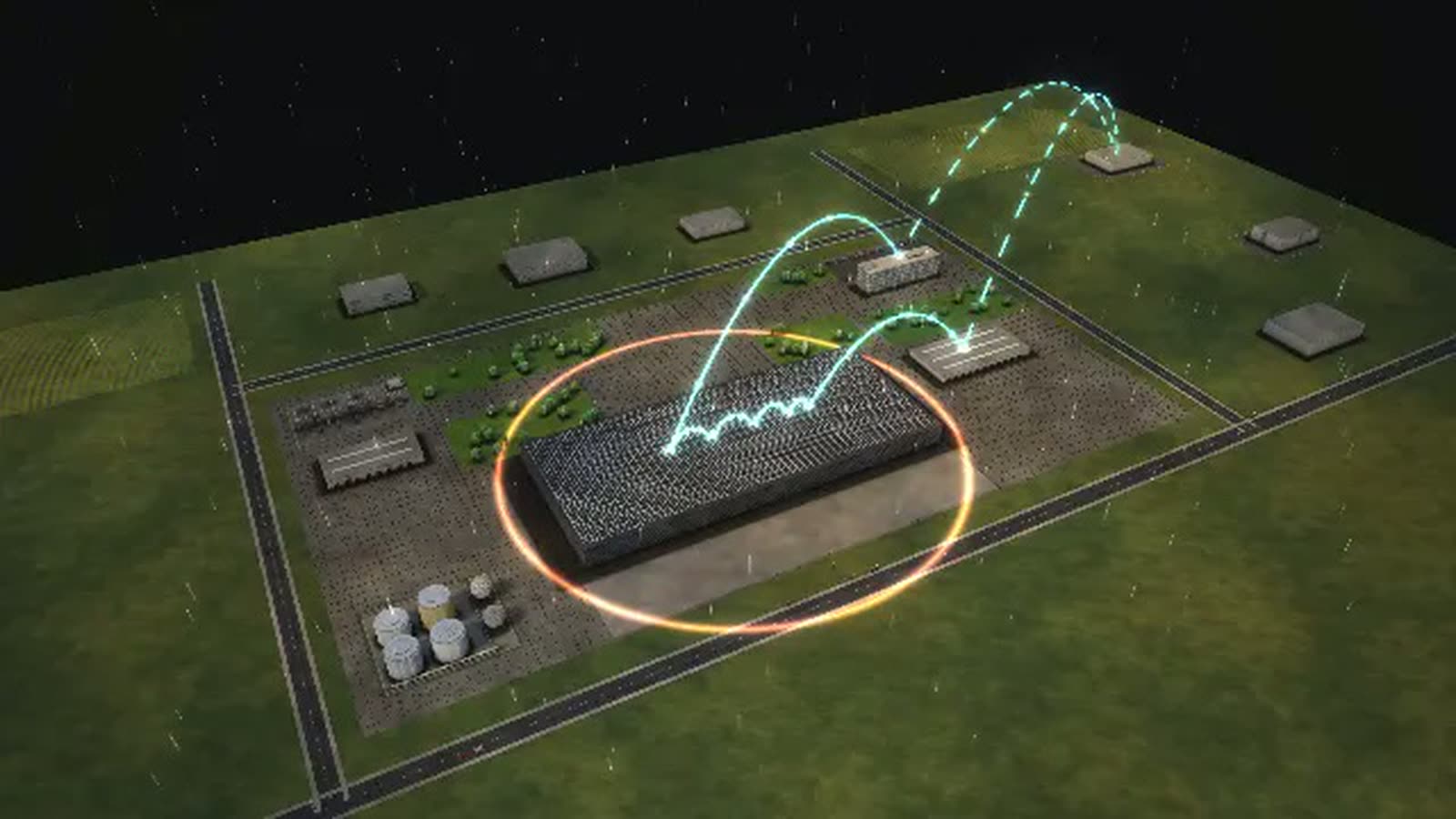
A chip fab as a walkable model: see where a wafer lot spends its weeks and why lithography sets the pace for the whole fab.
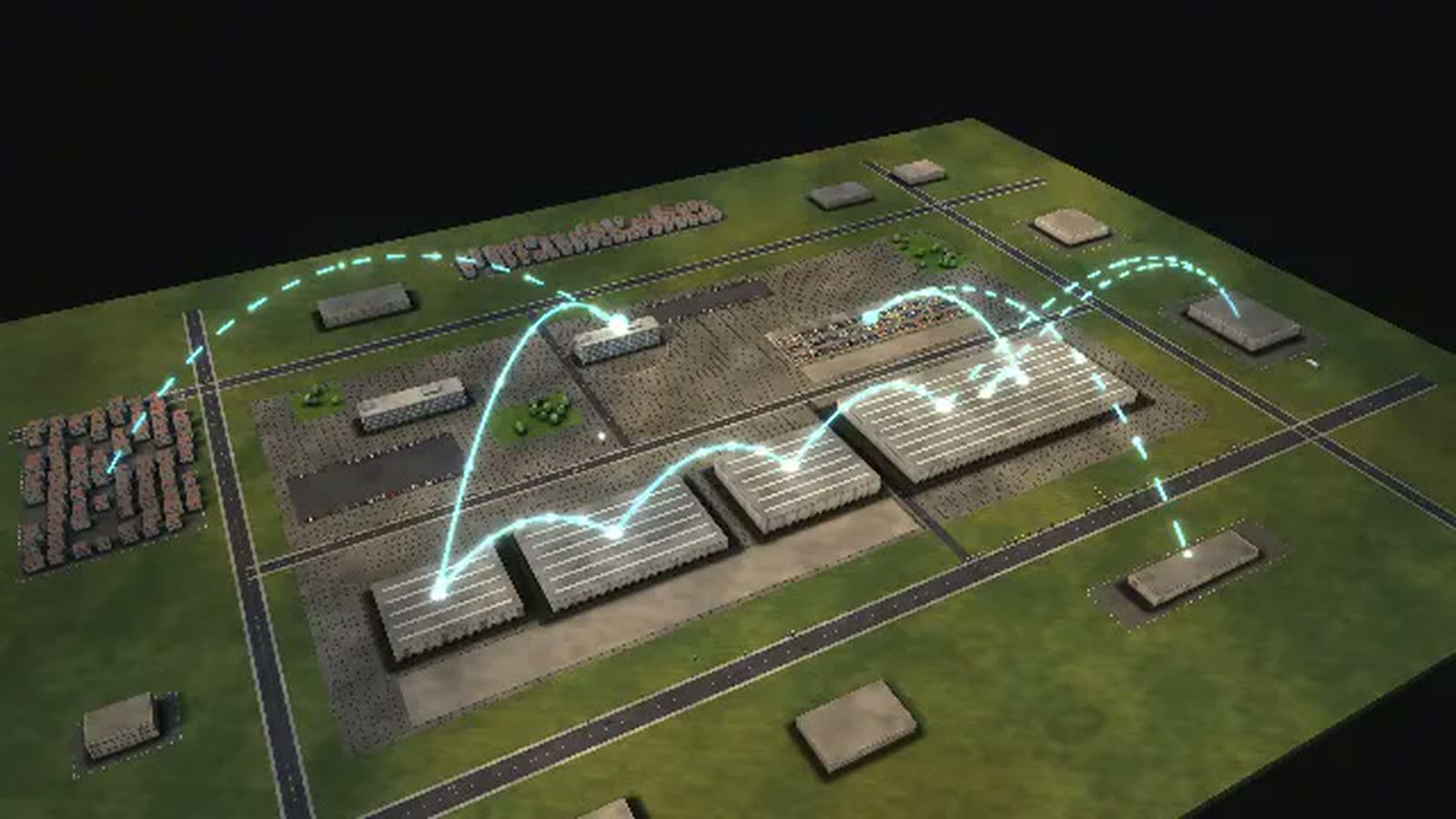
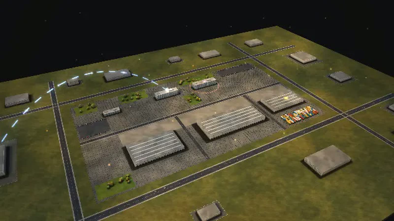
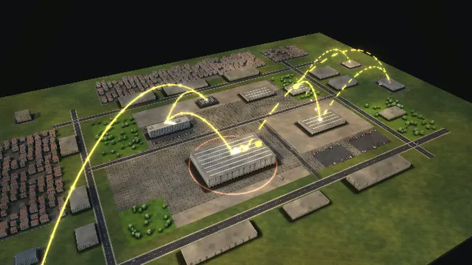
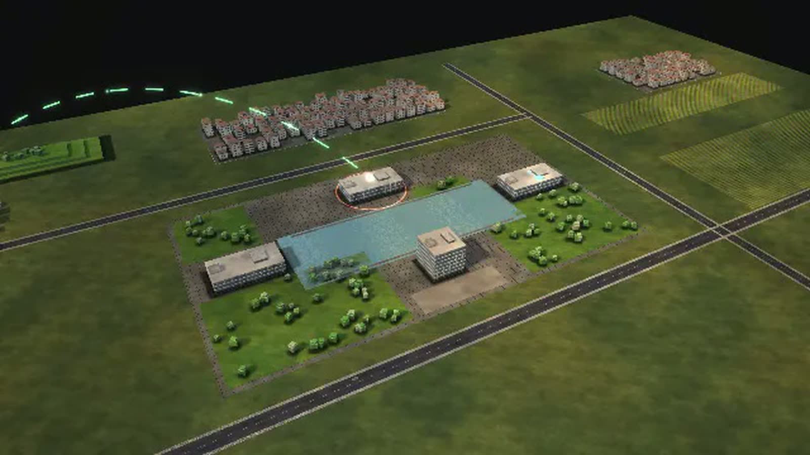
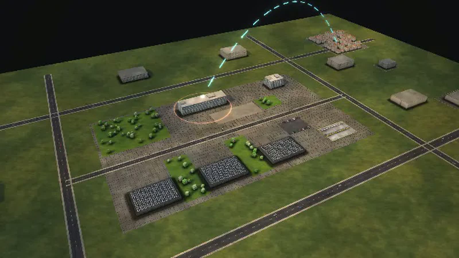
All data for LITHENA HALBLEITER are fictional. The model can be fitted to your fab's real data and filled with information that is not visible anywhere today – for example actual lot moves from your MES or maintenance windows for each lithography tool.
This page shows a semiconductor fab process simulation, using the fictional chipmaker LITHENA HALBLEITER. A lot of 25 wafers passes five times through the same loop of exposure, etch, deposition and polishing. The diagram ‘Where the time goes’ makes it plain: most of the time, the lot is waiting between tools.
The main process in one sentence: fab planning releases a lot, wafer test measures every chip after the fifth loop, then the wafers fly to an overseas assembler for packaging and final test before the chips ship to the customer. The model's target: in wafer test within nine weeks.
Lithography is the bottleneck. More wafer starts make the queue in front of it grow for weeks, and an extra tool is the most expensive lever in the fab. The page is written for fab managers, production control and capital planning, and for anyone who has to explain how a fab works to new hires, customers or policymakers.
A lot of wafers runs through the fab
- 01
Release lot (25 wafers): Fab planning releases a lot of 25 wafers.
- 02
Exposure: Layers 1–12: transistors: exposure.
- 03
Etch and clean: Layers 1–12: transistors: etch and clean.
- 04
Deposit and implant: Layers 1–12: transistors: deposit and implant.
- 05
Polish and measure: Layers 1–12: transistors: polish and measure.
- 06
Waiting and transport between tools: The lot waits in wafer boxes for the next tools.
- 07
Again: Exposure: Layers 13–24: contacts: exposure.
- 08
Again: Etch and clean: Layers 13–24: contacts: etch and clean.
- 09
Again: Deposit and implant: Layers 13–24: contacts: deposit and implant.
- 10
Again: Polish and measure: Layers 13–24: contacts: polish and measure.
- 11
Again: Waiting and transport between tools: The lot waits in wafer boxes for the next tools.
- 12
Again: Exposure: Layers 25–36: lower metal: exposure.
- 13
Again: Etch and clean: Layers 25–36: lower metal: etch and clean.
- 14
Again: Deposit and implant: Layers 25–36: lower metal: deposit and implant.
- 15
Again: Polish and measure: Layers 25–36: lower metal: polish and measure.
- 16
Again: Waiting and transport between tools: The lot waits in wafer boxes for the next tools.
- 17
Again: Exposure: Layers 37–48: upper metal: exposure.
- 18
Again: Etch and clean: Layers 37–48: upper metal: etch and clean.
- 19
Again: Deposit and implant: Layers 37–48: upper metal: deposit and implant.
- 20
Again: Polish and measure: Layers 37–48: upper metal: polish and measure.
How a semiconductor manufacturer can use the model
-
Internal communication
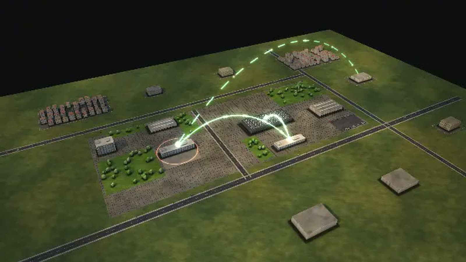
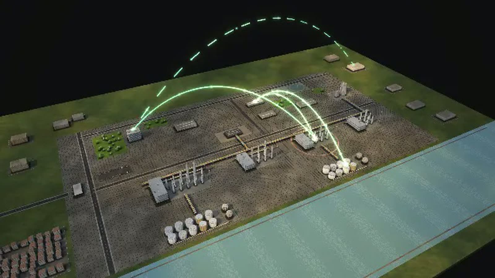
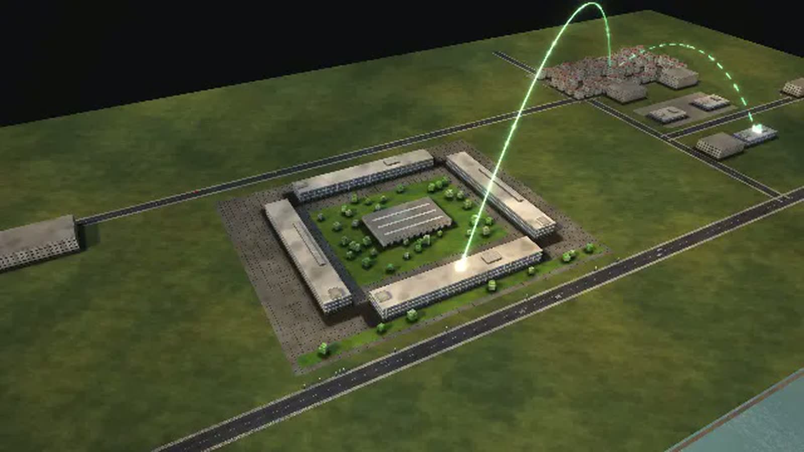
The whole fab in one picture: lithography, etch, deposition, metrology, wafer test and utilities across six buildings. The collaboration view draws arcs between the departments that work together, from the cleanroom to customer engineering.
For whomManagement, communications, all departments
-
Onboarding
New hires follow a lot through all five loops to wafer test and see where their tool sits in the chain. An eight-step guided tour explains the controls on the first visit.
For whomNew staff in the fab, equipment engineering and customer engineering
-
Training
Apprentices and students push wafer starts to full load, trigger cleanroom contamination and watch the queue in front of lithography grow – without touching a real tool.
For whomApprentices, work-study students, process and equipment technicians
-
Explaining to customers
Customers see the path of their lot: release, five loops, wafer test, overseas packaging, final test. It shows why a chip takes weeks and what a second assembler would change.
For whomAutomotive, industrial and electronics customers, sales, customer engineering
-
Strategic overview
‘What each control does’ ranks wafer starts, lithography tools, predictive maintenance and a second assembler by their effect on cycle time. A voltage dip shows how much the fab depends on the grid.
For whomExecutive team, controlling, capital planning, risk management
What is shown – why – for whom
| What is shown | Why | For whom |
|---|---|---|
| Diagram ‘Where the time goes’ for one lot | Whyshows that a wafer spends most of its time waiting | For whomProduction control, fab management |
| Queue in front of lithography in the resources view | Whyshows the fab's most expensive bottleneck | For whomFab management, capital planning |
| Diagram ‘What each control does’: wafer starts, lithography, maintenance, second assembler | Whyranks the levers by their effect on cycle time | For whomExecutive team, controlling |
| Diagram ‘What the work depends on’: ultrapure water, gases, substation | Whyshows how the fab depends on its utilities | For whomFacility management, risk management |
| Five passes through the same loop in the processes view | Whyexplains why a lot keeps returning to the same tools | For whomOnboarding, customers |
| Disruption ‘Voltage dip in the grid’ | Whyshows twelve hours of restart after a brief dip | For whomEnergy supply, site policy |
| Diagram ‘How a case flows’ to the overseas assembler | Whymakes the path across continents visible | For whomCustomers, supply chain |
Departments in the model
-
Management
Leads the fab and customer service.
-
Fab planning and dispatching
Releases lots and sets the sequence at the tools.
-
Lithography
Exposes every layer – the most expensive tools in the fab.
-
Etching and cleaning
Transfers the pattern into the layer.
-
Deposition and implantation
Deposits layers and dopes.
-
CMP and metrology
Polishes, measures, decides: continue or rework.
-
Equipment engineering
Keeps the tools running.
-
Utilities (ultrapure water, gases, power)
Without utilities the cleanroom stops.
-
Wafer test
Measures every chip on the wafer.
-
Yield engineering
Every point of yield is profit.
-
Failure analysis
Hunts defects under the microscope.
-
Process technology
Develops the layer recipes.
-
Customer engineering
Brings customer designs into the fab.
-
Sales
Sells capacity, commits dates.
-
Environment, health, safety
Gases, chemicals, wastewater.
-
Manufacturing execution (MES)
Knows every lot and every step.
All processes in the model
A lot of wafers runs through the fab
- 01Release lot (25 wafers): Fab planning releases a lot of 25 wafers.
- 02Exposure: Layers 1–12: transistors: exposure.
- 03Etch and clean: Layers 1–12: transistors: etch and clean.
- 04Deposit and implant: Layers 1–12: transistors: deposit and implant.
- 05Polish and measure: Layers 1–12: transistors: polish and measure.
- 06Waiting and transport between tools: The lot waits in wafer boxes for the next tools.
- 07Again: Exposure: Layers 13–24: contacts: exposure.
- 08Again: Etch and clean: Layers 13–24: contacts: etch and clean.
- 09Again: Deposit and implant: Layers 13–24: contacts: deposit and implant.
- 10Again: Polish and measure: Layers 13–24: contacts: polish and measure.
- 11Again: Waiting and transport between tools: The lot waits in wafer boxes for the next tools.
- 12Again: Exposure: Layers 25–36: lower metal: exposure.
- 13Again: Etch and clean: Layers 25–36: lower metal: etch and clean.
- 14Again: Deposit and implant: Layers 25–36: lower metal: deposit and implant.
- 15Again: Polish and measure: Layers 25–36: lower metal: polish and measure.
- 16Again: Waiting and transport between tools: The lot waits in wafer boxes for the next tools.
- 17Again: Exposure: Layers 37–48: upper metal: exposure.
- 18Again: Etch and clean: Layers 37–48: upper metal: etch and clean.
- 19Again: Deposit and implant: Layers 37–48: upper metal: deposit and implant.
- 20Again: Polish and measure: Layers 37–48: upper metal: polish and measure.
A customer brings a new chip
- 01Take over and check the design: Customer engineering takes over the finished design and checks it against the fab rules.
- 02Make photomasks: A photomask is made for every layer.
- 03First wafers as hot lot: The first wafers run through the fab as a hot lot.
- 04Customer checks the first chips: The customer brings up the first chips.
- 05Release to volume: Release to volume.
- 06In volume.
Yield drops
- 01Yield drops in test: In wafer test suddenly more chips fail.
- 02Failure analysis: defect map: Failure analysis overlays a defect map: it points to an etch tool.
- 03Hold the tool, stop lots: The tool is put on hold, affected lots are stopped.
- 04Fix the cause: Equipment engineering looks for the cause.
- 05Equipment maker service: The maker's service arrives.
- 06Release the tool again: Test wafers run, the tool is released.
- 07Inform customers: Customer engineering informs affected customers.
- 08Fixed.
What you can change
Controls
- Wafer starts: More lots in the fab: queues before lithography grow.
- Lithography tools: The most expensive lever in the fab.
- Predictive maintenance: Tool sensor data: fewer excursions (model assumption).
- Second assembler: Two assemblers: less waiting for packaging (model assumption).
Disruptions
- Cleanroom contamination: For two days only half the tools work until cleaned.
- Voltage dip in the grid: For twelve hours the tools restart after a voltage dip.
- Demand wave: For two months all customers want more.
- Manufacturing execution fails: For two hours no lot can be released or held.
What the model gives a chipmaker
-
01
Waiting made visible
In a fab, cycle time is mostly waiting time. The model calculates it live and shows it as the largest block in the diagram – clearer than any spreadsheet.
-
02
A bottleneck you can test
Raise wafer starts and the queue in front of lithography grows; add a tool and see what changes. The simulation keeps running while you move the controls.
-
03
The fab and its utilities
Ultrapure water, gas and chemical storage and the substation are buildings of their own. A grid disruption shows how long the tools take to come back.
-
04
Fourteen diagrams, one model
Cycle time, utilisation, supply chain and org chart are calculated live from the same simulation, in four groups. Nobody has to update a slide by hand.
-
05
Browser or big screen
The model runs in the browser and on large projections, for customer visits or a staff meeting. A demo mode plays everything on its own.
Basis and limits
Fictional semiconductor manufacturer · model based on researched industry structures · no forecast for real companies
1 case = 1 lot (25 wafers), 1 new chip or 1 yield excursion · 1 figure ≈ 20 employees
All volumes, durations, rates and capacities are model assumptions, not values of a real fab.
Twelve mask layers each are bundled into one pass; waiting between tools is combined into one station.
Documented: cycle time of about twelve weeks with hundreds of steps, lithography as the bottleneck, packaging and final test often at other firms in other regions.
Public sources the model is based on:
- SIA/BCG: Strengthening the Global Semiconductor Supply Chain
- SIA: why ramping up production takes time
- SemiEngineering: Battling Fab Cycle Times
- EU Chips Act, VO (EU) 2023/1781
Your fab as a model
Tell us about your fab: which data exist, which questions the model should answer and who will work with it. The password for the simulation comes by email once you ask for it.
cube4tec.de/spiele/minimal-organization/
Ask about this
Minimal Organization: Halbleiterhersteller
Similar business models
-
Pharmaceutical company
A pharmaceutical plant as a walkable model: follow a batch from the cleanroom to certification by the qualified person and see where the four weeks go.
-
Chemical group with integrated site
A chemical site as a walkable model: see how a polyethylene order runs through the integrated site and which plants stall when the cracker trips.
-
Smartphone maker
A smartphone maker without its own factory as a walkable model: repairs, spare parts, supply chain and product launch in a running simulation.
-
Car manufacturer
A car plant as a walkable model: follow an ordered car through the fixed build sequence and see what happens when the paint shop stops.
-
Special machine builder
A family-owned special machine builder as a walkable model: how a custom packaging line moves from enquiry to site acceptance and where the 28 weeks go.
-
Online retail
An order from click to doorstep as a walkable model: payment check, warehouse, packing, trucks, sortation and delivery in a running simulation.
-
Search engine
A search and advertising group as a walkable model: auctions in milliseconds, experiments over weeks, and a new ad campaign that waits for people.
-
Cloud provider
A cloud provider as a walkable model: support cases, zone outages and new data centres on three time scales, in a running simulation.
All data for LITHENA HALBLEITER are fictional. The model can be fitted to your fab's real data and filled with information that is not visible anywhere today – for example actual lot moves from your MES or maintenance windows for each lithography tool.